|
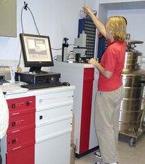
SQUID (Superconducting quantum interference device) Magnetometer with variable temperature platform (1.4K-800K)
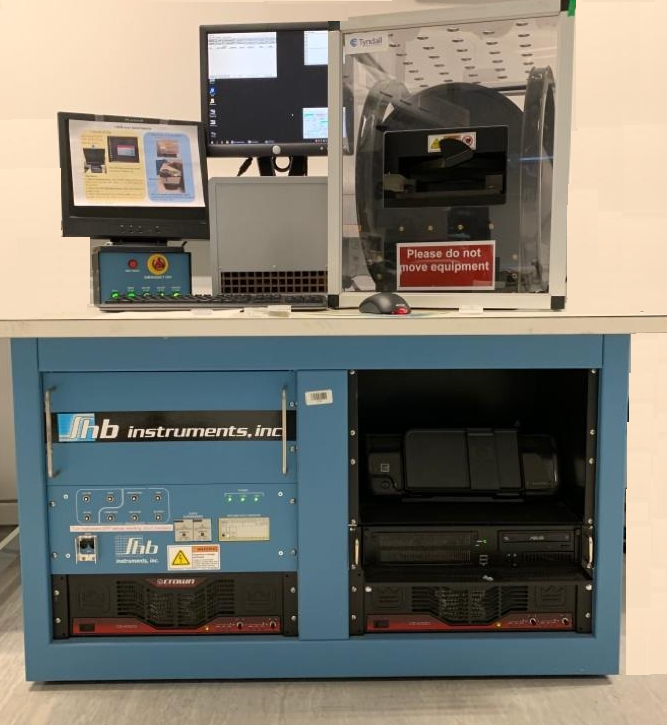
Wafer-Level (4” & 6”) Magnetic Hysteresis Loop Tracer
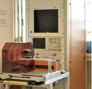
Ryowa complex permeability spectra
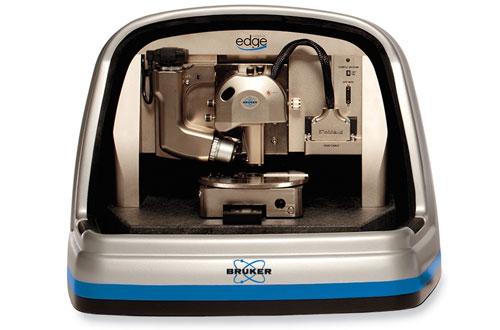
Magnetic Force Microscopy
|

|
|
|
|
|
SQUID (Superconducting quantum interference device) Magnetometer with variable temperature platform (1.4K-800K)
Wafer-Level (4” & 6”) Magnetic Hysteresis Loop Tracer
Ryowa complex permeability spectra
Magnetic Force Microscopy
|